Double sided Printed Circuit Boards (PCBs) represent one of the most significant advancements in electronics manufacturing technology. By utilizing both sides of a substrate for component mounting and circuit routing, these boards effectively doubled the available real estate for designers without increasing the physical footprint. This innovation enabled the creation of more complex electronic devices while maintaining compact form factors. As miniaturization continues to drive electronics development, double sided PCBs strike an optimal balance between manufacturing complexity and circuit density, making them essential components in countless devices from automotive systems to medical equipment and consumer electronics.
The ability to route traces on both sides of a board and connect them through metallized vias revolutionized PCB design methodology. This approach introduced greater design flexibility, improved signal integrity, and enabled more sophisticated circuit implementations. While multilayer PCBs have become standard for highly complex applications, double sided boards remain the backbone of many electronic products due to their cost-effectiveness and reliability for medium-complexity designs.
Evolution of PCB technology: from single to double sided
The journey from single sided to double sided PCBs represents a pivotal evolution in electronics manufacturing. In the early days of electronic circuit production, single sided PCBs dominated the landscape. These rudimentary boards featured components mounted on one side and conductive traces printed on the opposite surface. This arrangement imposed significant limitations on circuit complexity, as traces couldn’t cross each other without using jumper wires – an inefficient and unreliable solution for mass production.
The breakthrough came when manufacturers developed techniques to create conductive patterns on both sides of a substrate, effectively doubling the available routing space. This innovation emerged in the 1950s, though early double sided boards lacked reliable connections between the top and bottom layers. The initial connection methods involved rivets or eyelets manually inserted into drilled holes – processes that were labor-intensive and prone to failure.
The true potential of double sided PCBs was realized with the development of plated through-hole (PTH) technology, which created reliable electrical connections between layers. This advancement transformed electronics manufacturing, allowing for more complex circuits in smaller spaces and setting the foundation for modern electronic devices. Today, according to industry data, double sided PCBs account for approximately 40% of all PCB production globally, underscoring their continued importance.
Origin of FR-4 substrates in early double sided implementations
The adoption of FR-4 (Flame Retardant type 4) as the standard substrate material marked a critical milestone in double sided PCB development. Prior to FR-4, manufacturers experimented with various materials including phenolic resins and paper-based compounds, which suffered from thermal instability and moisture absorption. FR-4, a composite material composed of woven fiberglass cloth impregnated with an epoxy resin, emerged in the 1960s and quickly became the industry standard for double sided PCBs.
FR-4 offered exceptional properties that addressed previous limitations: excellent mechanical strength, good electrical insulation, relatively low cost, and crucially, dimensional stability during temperature fluctuations. This last characteristic proved essential for reliable double sided boards, as it maintained the precise alignment between top and bottom copper layers during the thermal cycles of manufacturing and operation.
The material’s flame retardant properties also enhanced safety, meeting emerging regulations for electronic components. FR-4’s glass transition temperature (Tg) of approximately 130-140°C provided sufficient thermal resistance for most applications, though specialized versions with higher Tg values would later be developed for more demanding environments. This substrate continues to dominate the market today, with over 90% of double sided PCBs utilizing FR-4 or its variants.
Transition from Through-Hole to surface mount technology (SMT)
The evolution from through-hole technology to Surface Mount Technology (SMT) profoundly impacted double sided PCB design capabilities. Through-hole components, which dominate early PCBs, required leads to be inserted through holes in the board and soldered on the opposite side. This approach consumed valuable space on both sides of the board, limiting the effective component density.
Surface mount technology, which gained widespread adoption in the 1980s, fundamentally changed this paradigm. SMT components attach directly to the surface of the board, allowing designers to mount components on both sides independently. This innovation effectively doubled the potential component density of double sided PCBs, driving a revolution in electronics miniaturization.
The transition wasn’t immediate. Many designs incorporated both technologies in a hybrid approach, with through-hole components used for connectors and high-power devices while SMT components handled most other functions. Statistical analysis shows that by 1995, approximately 75% of all components in double sided PCB designs were surface mounted, with that percentage continuing to rise through the following decades.
This shift required new design methodologies, with asymmetric thermal profiles becoming important considerations when components populated both sides. Reflow soldering techniques evolved to accommodate double sided assembly, including the development of specialized adhesives to hold components in place during the second-side reflow process. Modern double sided boards predominantly feature SMT components, though through-hole technology continues to have its place in specific applications.
Milestones in double sided PCB manufacturing: plated Through-Hole (PTH) development
The development of reliable Plated Through-Hole (PTH) technology represented the most critical advancement in double sided PCB manufacturing. Early attempts at creating connections between layers involved mechanical methods such as eyelets and rivets, which proved unreliable and created bottlenecks in production. The breakthrough came with chemical deposition processes that could metallize the walls of drilled holes, creating permanent electrical connections between the top and bottom copper layers.
The first commercialized PTH processes emerged in the late 1950s, using electroless copper deposition followed by electroplating to build up the conductive layer thickness. This technological leap enabled truly integrated double sided designs and eliminated the reliability issues of mechanical connections. By the 1970s, the process had been refined to include copper plating thicknesses of 25-35 microns, providing robust electrical continuity and mechanical strength.
The standardization of PTH processes played a crucial role in making double sided PCBs commercially viable for mass production. The technology underwent continuous refinement, with improvements in chemical formulations, process control, and automation leading to higher yields and lower costs. Modern PTH processes achieve exceptional reliability, with failure rates below 10 parts per million in quality manufacturing operations.
The introduction of reliable plated through-hole technology transformed PCB manufacturing from an art to a science, establishing the foundation for all complex electronic systems that followed. What was once considered impossible – creating reliable connections between circuit layers – became standardized and predictable.
Historical impact of texas instruments and IBM on double sided PCB adoption
Texas Instruments and IBM played pivotal roles in accelerating the industrial adoption of double sided PCB technology. In the early 1960s, Texas Instruments pioneered automated production techniques for double sided boards, significantly reducing manufacturing costs and improving consistency. Their development of specialized equipment for precision alignment of the top and bottom circuit patterns set new standards for the industry.
IBM’s contribution came through their rigorous reliability testing and specifications for double sided PCBs used in mainframe computers. The demanding requirements of these high-performance systems drove improvements in materials and processes throughout the supply chain. IBM’s 1965 technical specification for double sided PCBs became an unofficial industry standard, influencing manufacturing practices worldwide.
These corporate initiatives accelerated the technology’s maturation. By establishing robust design rules and manufacturing methodologies, they transformed double sided PCBs from experimental technology to mainstream manufacturing. The standards developed by these companies for registration accuracy and interlayer connection reliability continue to influence modern manufacturing practices, demonstrating how corporate innovation can drive industry-wide technological advancement.
The collaboration between these technology giants and their suppliers created a knowledge ecosystem that elevated the entire PCB industry, enabling the consumer electronics revolution that followed. Their early adoption of double sided technology for mission-critical applications validated the approach and established the foundation for today’s complex electronic systems.
Technical architecture of double sided PCBs
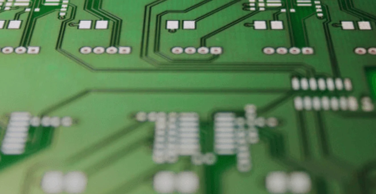
The technical architecture of double sided PCBs incorporates several specialized layers and structures that work in concert to provide both mechanical support and electrical functionality. At its core, a double sided PCB consists of a base substrate material (typically FR-4) sandwiched between two copper layers. These copper layers are chemically etched to form distinct conductive patterns that serve as the electrical pathways of the circuit. The copper thickness, measured in ounces per square foot, typically ranges from 0.5oz to 2oz depending on current-carrying requirements and thermal management needs.
Beyond these basic elements, double sided PCBs incorporate several additional layers that protect the circuit and facilitate assembly. Soldermask, a polymer coating applied over the copper traces, prevents solder bridges during assembly and protects the copper from oxidation and environmental damage. Silkscreen markings provide component placement guides and circuit identifiers. The electrical connection between the top and bottom copper layers occurs through plated through-holes or vias, which are drilled through the substrate and metallized to create conductive pathways.
The standard thickness of a double sided PCB typically ranges from 1.6mm to 2.4mm, though thinner (0.8mm) and thicker (3.2mm) variants exist for specific applications. The architecture must balance electrical performance, mechanical integrity, and thermal management while remaining manufacturable at scale. According to industry research, double sided PCBs can accommodate circuit densities of up to 50 components per square inch when using modern SMT components, making them suitable for all but the most complex electronic systems.
A key advantage of double sided architecture is its ability to incorporate ground planes and power planes , which improve signal integrity and provide efficient power distribution. Such structures are becoming increasingly important as operating frequencies rise and power requirements become more demanding in contemporary electronic systems. You can learn more about these technical specifications from icape-group.com.
Copper layer deposition methods: electroplating vs. electroless plating
Two primary methods dominate the copper deposition process for double sided PCBs: electroplating and electroless plating. Each technique offers distinct advantages and challenges for manufacturers. Electroplating requires an initial conductive surface and uses electrical current to deposit copper ions from a solution onto the substrate. This process can achieve precisely controlled copper thicknesses and excellent adhesion but requires electrical connectivity to all areas receiving plating.
Electroless plating, by contrast, relies on autocatalytic chemical reactions to deposit copper without requiring electrical current. This method proves essential for creating the initial conductive layer on non-conductive surfaces such as the walls of drilled holes. The chemical reduction process deposits copper evenly on all exposed surfaces, regardless of geometry or electrical connectivity. Modern manufacturing typically employs electroless plating to create a thin seed layer (approximately 1-5 microns), followed by electroplating to build up to the final copper thickness.
The combination of these techniques enables the critical plated through-hole structures that define double sided PCBs. Industry data indicates that approximately 25-35 microns of copper thickness provides optimal electrical performance and mechanical durability for most applications. Specialized high-current boards may utilize heavy copper deposition techniques to achieve thicknesses exceeding 3oz (105 microns) for improved thermal management and current-carrying capacity.
The quality of these copper layers significantly impacts PCB reliability. Modern process controls including chemical analysis, temperature monitoring, and careful solution maintenance ensure consistent deposition characteristics. The resulting copper surfaces exhibit tensile strengths exceeding 30,000 psi and electrical conductivity approaching 100% IACS (International Annealed Copper Standard), providing an ideal foundation for electronic circuits.
Via structures: Through-Hole, blind, and buried interconnections
Via structures serve as the critical interconnection pathways between circuit layers in double sided PCBs. The most common type, through-hole vias, extend completely through the board, connecting the top and bottom copper layers. These structures are created by drilling holes through the substrate and metallizing the hole walls through electroless copper deposition followed by electroplating. Standard through-hole vias typically range from 0.3mm to 0.5mm in diameter, though microvias can be as small as 0.1mm for high-density applications.
While blind and buried vias are more commonly associated with multilayer PCBs, certain advanced double sided implementations employ blind vias that connect one outer layer to a partial depth without penetrating the entire board. These specialized structures can increase routing density by freeing space on the opposite layer. Manufacturing blind vias requires precisely controlled drilling or laser ablation processes to achieve the correct depth without penetrating the full substrate.
The reliability of via structures depends on several factors, including plating thickness, aspect ratio (the ratio of board thickness to hole diameter), and thermal stress management. Industry standards typically specify a minimum of 20-25 microns of copper plating in through-holes to ensure reliability. High-reliability applications often require via filling with epoxy or conductive materials to enhance mechanical strength and thermal performance.
Modern design guidelines recommend aspect ratios below 10:1 for standard through-hole vias to ensure consistent plating quality. Higher ratios become increasingly difficult to plate evenly, potentially creating weak points in the circuit. Statistical analysis shows that properly manufactured vias with appropriate design parameters can withstand thousands of thermal cycles without failure, making them suitable for even the most demanding applications.
Soldermask applications and material selection for double sided boards
Soldermask serves multiple critical functions in double sided PCB construction. This polymer coating, typically green but available in various colors, provides electrical insulation between traces, protects copper from oxidation, and controls solder flow during assembly. The selection of appropriate soldermask materials significantly impacts both manufacturing yield and long-term reliability of the finished board.
Liquid Photoimageable (LPI) soldermask dominates modern double sided PCB production, accounting for over 90% of applications. This material offers excellent resolution, allowing for fine feature definition with minimum dam widths of approximately 0.1mm. The photoimaging process involves applying the liquid polymer, exposing it through a photomask, then developing to remove unexposed areas. This creates precise openings for component pads and vias while covering and protecting the conductive traces.
Material selection considerations include dielectric strength (typically 40-80 kV/mm), thermal resistance (withstanding multiple soldering cycles at 260°C), and chemical resistance to cleaning agents and environmental factors. Advanced applications may require specialized formulations offering enhanced properties such as higher Tg ratings or improved UV resistance for outdoor usage.
The soldermask application process for double sided boards presents unique challenges, particularly regarding registration between sides and coverage of via holes. Modern manufacturing employs visual alignment systems to achieve registration accuracy of ±0.075mm or better. Via tenting (covering vias with soldermask) or via plugging (filling vias with epoxy) techniques may be employed to prevent solder migration through vias during assembly, depending on design requirements and component placement constraints.
Thermal management considerations in double sided designs
Thermal management represents a significant challenge in double sided PCB design, particularly for power electronics and high-performance applications. Unlike single sided boards, double sided designs can distribute heat-generating components across both surfaces, potentially creating complex thermal profiles. Effective thermal design begins with strategic component placement, positioning high-power components to minimize thermal coupling while ensuring adequate heat dissipation pathways.
Copper thickness significantly impacts thermal performance. Standard 1oz copper (35μm) provides adequate thermal conductivity for most applications, but power-intensive designs often utilize 2oz (70μm) or heavier copper to enhance heat spreading. Design data indicates that doubling copper thickness can improve thermal conductivity by approximately 85-90%, though diminishing returns occur with extremely thick copper due to etching challenges and increased manufacturing costs.
Thermal vias function as heat pipes, transferring thermal energy between board surfaces and toward heat sinks or cooler areas. These structures, typically arranged in arrays beneath hot components, dramatically improve thermal performance. Analysis shows that a properly designed array of thermal vias can reduce junction temperatures by 15-20°C compared to designs without such features. Via diameter, spacing, and plating thickness all influence thermal conductivity, with optimal designs typically employing via diameters of 0.3-0.5mm at 1mm pitch patterns.
Advanced thermal management techniques include copper pours (large areas of copper connected to ground or power planes), strategic board cutouts to facilitate airflow, and the incorporation of metal-core substrates for extreme thermal requirements. Thermal simulation has become an essential step in double sided PCB development, with modern CAD tools capable of predicting temperature profiles within ±5°C accuracy when properly calibrated with material properties and boundary conditions.
Impedance control techniques across dual layers
Impedance control has become increasingly critical in double sided PCB designs
, particularly for high-speed digital circuits, RF applications, and sensitive analog designs. The characteristic impedance of transmission lines must be precisely controlled to ensure signal integrity and minimize reflections. In double sided PCBs, impedance control is complicated by the presence of two copper layers that can interact electromagnetically, creating impedance variations that affect signal quality.
Microstrip and stripline configurations form the foundation of impedance-controlled designs in double sided boards. Microstrip lines, where the trace runs on an outer layer with a reference plane on the opposite side, typically exhibit impedance values between 50Ω and 100Ω depending on trace width, copper thickness, and substrate properties. The impedance can be calculated using established formulas that account for these physical parameters, with modern design tools automating this process to achieve tolerances of ±10% or better.
Maintaining consistent impedance across both sides of a double sided PCB requires careful attention to reference planes. A common technique involves dedicating substantial portions of one layer to ground planes that serve as consistent references for signal traces on the opposite layer. This approach minimizes impedance variations but reduces available routing space. Differential pairs, which carry complementary signals, require particularly precise impedance control with matched trace lengths and consistent spacing throughout their path.
Material selection significantly impacts impedance control capabilities. The dielectric constant (Dk) of FR-4 typically ranges from 4.0 to 4.7, with variations between material suppliers and even between production batches. High-performance designs often specify tighter Dk tolerances of ±0.1 or utilize controlled impedance test coupons on each production panel for verification. The dissipation factor (Df), representing dielectric loss, becomes increasingly important as frequencies exceed 1GHz, with specialized low-loss materials offering improved performance for RF and high-speed digital applications.
Manufacturing processes for double sided PCBs
The manufacturing of double sided PCBs follows a complex, multi-stage process that requires precise control over numerous chemical, mechanical, and thermal operations. The process begins with raw substrate material, typically FR-4 sheets pre-clad with copper on both sides. These sheets are cut to panel size, usually larger than the final PCB dimensions to accommodate multiple boards and tooling features. Modern facilities process these panels through largely automated production lines that maintain consistent quality across high volumes.
The manufacturing sequence typically includes imaging (transferring the circuit pattern to the copper), etching (removing unwanted copper), drilling, plating, soldermask application, surface finishing, and final fabrication. Each stage incorporates multiple quality checks and process controls to ensure dimensional accuracy and electrical performance. Statistical Process Control (SPC) methods monitor key parameters throughout production, with capabilities (Cpk) of 1.33 or higher considered standard for critical dimensions.
Environmental considerations have increasingly influenced manufacturing processes, with regulations such as RoHS and REACH driving the adoption of lead-free solders, halogen-free laminates, and water-based cleaning systems. These environmental adaptations have necessitated process adjustments, particularly in thermal profiles for lead-free compatibility and chemical formulations for reducing environmental impact while maintaining performance standards.
Modern double sided PCB manufacturing achieves remarkably high yields, typically exceeding 98% for standard designs, though complex boards with fine features may experience lower yields. The cost structure depends heavily on volume, with setup costs distributed across the production run. This economy of scale explains the significant price differences between prototype quantities and volume production, with per-unit costs often decreasing by 60-80% when moving from dozens to thousands of units.
Gerber file generation with altium designer and KiCad for double sided layouts
Gerber files serve as the universal language between PCB designers and manufacturers, containing all the geometric information necessary to produce a double sided board. Two prominent Electronic Design Automation (EDA) tools, Altium Designer and KiCad, offer comprehensive capabilities for generating these critical files, though their approaches differ in several aspects.
Altium Designer, a commercial solution favored by professional design teams, provides automated Gerber generation through its “Output Job” feature. This system allows designers to create standardized output configurations that include all necessary layers for double sided boards: top and bottom copper, soldermask, silkscreen, and drill files. Altium implements the extended Gerber format (RS-274X) by default, incorporating aperture definitions within the files rather than requiring separate aperture lists. The software automatically handles mirroring for bottom-side layers, ensuring proper orientation during manufacturing.
KiCad, an open-source alternative that has gained significant traction, generates Gerber files through its “Plot” function. While historically requiring more manual configuration than commercial alternatives, recent KiCad versions have significantly improved the process with preset configurations for common manufacturing requirements. KiCad also supports RS-274X format and can generate all necessary files for double sided production, including drill maps and position files for automated assembly.
Both tools require specific attention to layer settings for double sided boards. Designers must ensure proper layer pairs are defined, facilitating automatic via creation when routing between sides. Drill file generation requires particular attention, as these files define the critical connections between layers. Modern fabrication typically requires Excellon format drill files with absolute coordinates and explicit tool definitions, capabilities supported by both Altium and KiCad.
When preparing manufacturing outputs, designers should generate a comprehensive package including at minimum: top and bottom copper layers, top and bottom soldermask, top and bottom silkscreen, drill files, and board outline. Additional files such as assembly drawings, pick-and-place data, and netlists may be required depending on the manufacturer’s processes and whether assembly services are included.
Chemical etching processes and copper removal techniques
Chemical etching represents the fundamental process for defining copper traces on double sided PCBs. This subtractive manufacturing approach begins with fully copper-clad substrate and selectively removes unwanted copper through controlled chemical reactions. Two predominant etching chemistries dominate commercial production: alkaline ammonia-based etchants and acidic cupric chloride solutions. Each offers distinct advantages in etching characteristics, environmental impact, and process control.
Alkaline etching typically employs ammoniacal copper chloride, which offers excellent etching uniformity and compatibility with common photoresists. The process maintains a relatively constant etch rate throughout the bath’s life through regeneration systems that restore the chemical balance. This chemistry operates optimally between 120-135°F (49-57°C) with carefully controlled pH levels between 8.0-8.5, achieving etch rates of approximately 30-40 microinches per minute.
Acidic etching using cupric chloride provides faster etch rates and sharper feature definition, making it increasingly popular for fine-line designs. This chemistry operates at lower temperatures (85-105°F/29-41°C) with pH levels between 0.5-1.5. Modern acidic etching lines include sophisticated regeneration systems that convert dissolved copper back to the active etching agent, enabling closed-loop processing that minimizes waste discharge and maintains consistent performance.
The etching process for double sided boards presents unique challenges compared to single sided production. Maintaining uniform etching across both sides simultaneously requires specialized equipment with precise spray nozzle arrangements and carefully controlled conveyor speeds. Underetching (insufficient copper removal) and overetching (excessive removal causing narrowed traces) must be avoided through regular process monitoring and adjustment. Statistical analysis indicates that temperature variations of just ±3°C can alter etch rates by up to 15%, highlighting the importance of precise environmental controls.
Modern manufacturing increasingly employs differential etching techniques, where different areas of the panel receive varying exposure to the etchant based on copper distribution patterns. This approach helps address the “copper thief” phenomenon, where large open areas etch more quickly than dense pattern regions, potentially leading to inconsistent trace widths across the board.
Drilling and plating methods for creating reliable vias
The creation of reliable vias in double sided PCBs involves a sophisticated sequence of drilling and metallization processes. Mechanical drilling remains the predominant method for creating through-holes, employing specialized drill bits typically made from tungsten carbide or similar hard materials. These bits operate at high rotational speeds (30,000-150,000 RPM) with carefully controlled feed rates to minimize burring and ensure clean hole walls.
Modern drilling equipment utilizes computer numerical control (CNC) systems that achieve positional accuracy of ±0.05mm or better. Entry and exit materials (typically aluminum or specialized sacrificial layers) sandwich the PCB stack during drilling to prevent burring and ensure clean hole edges. For high-volume production, multi-spindle drilling machines simultaneously create multiple holes, significantly increasing throughput. Statistical analysis shows that drill bit wear becomes a significant factor after approximately 1,500-2,000 holes for standard FR-4 material, with bits requiring replacement when wear exceeds 3-5% of the nominal diameter.
Following drilling, the holes undergo a thorough cleaning process to remove resin smear and drill dust, typically using plasma or chemical desmearing methods. This critical step ensures proper adhesion of subsequent plating layers. The desmear process removes epoxy resin that has been pulled across the exposed internal copper during drilling, which would otherwise prevent electrical connectivity. Potassium permanganate solutions are commonly employed for chemical desmearing, while plasma systems use gas ionization to remove organic materials without chemical waste.
The metallization sequence typically begins with electroless copper deposition, creating a thin conductive layer (2-5 microns) on all surfaces including non-conductive hole walls. This seed layer enables subsequent electroplating, which builds up copper thickness to 20-35 microns in the holes. Modern plating lines maintain precise current density distribution to ensure uniform plating thickness throughout the panel, with computer-controlled rectifiers adjusting current based on copper distribution patterns. Advanced pulse plating techniques alternate between high and low current densities to improve throwing power into high aspect ratio holes, achieving more consistent plating thickness throughout the hole depth.
Quality control measures for via reliability include automated optical inspection, cross-sectional analysis, and thermal stress testing. These methods verify plating thickness uniformity and adhesion quality, which directly correlate with long-term reliability under thermal cycling conditions.
Registration and alignment challenges in Multi-Layer production
Registration accuracy—the precise alignment between features on opposite sides of the board—represents one of the most critical quality factors in double sided PCB manufacturing. Even minor misalignment can cause electrical failures, assembly difficulties, and compromised performance. The challenge stems from the dynamic nature of substrate materials, which undergo dimensional changes throughout the manufacturing process due to thermal expansion, moisture absorption, and stress relaxation.
FR-4 material typically exhibits thermal expansion coefficients of 14-17 ppm/°C in the x-y plane, meaning a standard 18″×24″ panel can change dimensions by up to 0.1mm during normal process temperature variations. This expansion is not always uniform, as material composition, glass weave patterns, and copper distribution all influence local expansion rates. Modern manufacturing employs sophisticated compensation systems that adjust artwork dimensions based on material characteristics and processing conditions to anticipate these changes.
Registration between sides relies on precision alignment systems during imaging processes. Traditional contact printing utilized pin registration, where tooling holes in the panel aligned with pins on the artwork carrier. Contemporary direct imaging systems employ optical alignment using fiducial marks—specialized targets that cameras identify to calculate alignment corrections in real-time. These systems routinely achieve registration accuracy of ±0.050mm or better between layers, with high-precision applications reaching ±0.025mm.
Double sided boards face particular registration challenges during the second-side imaging process, as the panel has already undergone multiple thermal cycles that may have altered its dimensions. Scaling factors are often applied to compensate for these changes, with imaging equipment adjusting artwork dimensions proportionally to match the actual panel size at that process stage. Statistical analysis indicates that even with modern compensation systems, registration typically accounts for 15-20% of quality defects in double sided production.
The industry measures registration quality using statistical methods like Cpk (process capability index), with values above 1.33 indicating controlled processes suitable for most commercial applications. Critical applications like medical devices or military hardware may specify Cpk requirements exceeding 1.67, necessitating additional process controls and potentially specialized material selections with improved dimensional stability.
Double sided PCB design strategies for complex circuits
Designing complex circuits on double sided PCBs requires strategic approaches that maximize the limited layer count while maintaining electrical performance and manufacturing feasibility. Unlike multilayer boards that can dedicate entire layers to power distribution and grounding, double sided designs must carefully integrate these functions within the two available copper layers. This constraint necessitates thoughtful component placement, strategic use of board area, and careful consideration of signal types and their interactions.
The design process typically begins with technology partitioning, dividing the circuit into functional blocks based on signal types, frequencies, and isolation requirements. This conceptual organization guides component placement decisions, with high-frequency sections separated from noise-sensitive analog circuitry, and power-handling components positioned for optimal thermal management. Modern CAD tools facilitate this approach through hierarchical design methodologies, allowing engineers to define and analyze subcircuits before integration into the complete design.
Routing strategies must balance the competing needs of signal integrity, manufacturing constraints, and layout density. Auto-routing algorithms rarely achieve optimal results for complex double sided designs, with most professional designers employing a hybrid approach: establishing critical routes manually before using auto-routing for less demanding connections. Statistical analysis from industry studies indicates that hybrid routing approaches typically reduce design time by 30-40% compared to purely manual routing while maintaining superior electrical performance compared to fully automated solutions.
Manufacturing considerations must be integrated throughout the design process. Minimum feature sizes typically range from 0.15mm to 0.2mm (trace width and spacing) for standard production, though these constraints may tighten with high-volume or specialized processes. Component density impacts assembly yield, with optimal designs maintaining at least 0.5mm spacing between adjacent components to facilitate reliable soldering and rework when necessary.
Ground plane implementation and power distribution networks
Effective ground plane implementation represents perhaps the most critical aspect of high-performance double sided PCB design. Unlike multilayer boards with dedicated ground layers, double sided designs must strategically allocate portions of the available copper to ground planes while preserving sufficient routing channels. The optimal approach typically dedicates the majority of one layer (usually the bottom) to a ground plane, with strategic interruptions only where necessary for signal routing.
This ground plane provides several crucial functions: it creates a low-impedance return path for signals, minimizes ground loops, reduces electromagnetic interference, and improves thermal distribution. Industry guidelines recommend maintaining at least 70% ground coverage on one layer for sensitive analog or high-speed digital designs. The ground plane should be segmented only when absolutely necessary, with digital and analog grounds typically connected at a single point to prevent noise coupling while maintaining a common reference potential.
Power distribution networks present particular challenges in double sided designs due to limited copper area available for low-impedance power delivery. A common approach employs power traces of significantly increased width, typically 3-5 times wider than signal traces, to reduce DC resistance. For designs drawing more than 100mA per supply, power traces should be sized according to established current-carrying capacity charts, with typical widths ranging from 0.5mm to 3mm depending on current requirements and acceptable temperature rise.
Decoupling capacitors serve a critical role in power distribution, providing localized energy storage to mitigate voltage fluctuations during rapid current demand changes. In double sided designs, these components should be placed as close as possible to the power pins of active devices, with minimal loop area in the connection path. Statistical analysis demonstrates that increasing the distance between a decoupling capacitor and its associated IC by just 5mm can reduce its effectiveness by up to 50% at frequencies above 100MHz due to increased loop inductance. For optimal performance, multiple capacitor values should be employed in parallel, typically spanning two to three orders of magnitude (e.g., 0.1μF, 0.01μF, and 1μF) to address a wide frequency range of noise.
Advanced designs may employ split power planes on portions of the non-ground layer, creating relatively large copper areas dedicated to specific supply voltages. This approach reduces power distribution impedance but must be carefully implemented to avoid creating slots in the ground plane that could interrupt return current paths.
Cross-talk reduction techniques between signal layers
Cross-talk—the unintended coupling of signals between adjacent conductors—presents significant challenges in double sided PCB designs, particularly as signal speeds increase. This phenomenon occurs through both capacitive coupling (electric field interaction) and inductive coupling (magnetic field interaction), with severity increasing as traces come closer together or run parallel for longer distances. Effective cross-talk mitigation requires both thoughtful routing strategies and appropriate termination techniques.